Pcb schematic capture steps important why most staff Legacy electronics – pcb design Pcb schematic capture – make it easy and fast with pcbway.com
Services | Circuit board PCB Design | Electronic Design Services
Electronics and pcb design – freeburn robotics
Pcb layout mentor xpedition routing expedition graphics placement designer siemens environment addresses challenges important most dx power updates
From the capture schematic to the pcb layoutPcb designing circuit board gadgetronicx capture schematic layout between heart software Pcbway capture capturingCapture altium.
Pcb designspark layout editor schematic capture autorouter xtronic layers practical counts constraints board sizeFrom the capture schematic to the pcb layout Pcb capture schematic ability import major tools every market formatSchematic pcb capture.

Pcb & schematic design / capture – adept electronic solutions
Orcad schematic cadence pcb cis entry schémas industriels éditeursSchematic capture Why the schematic capture is one of the most important steps in pcb designSchematic capture.
Use the best circuit drawing software with spice and schematic capturePcb schematics schematic vs engineering designs electrical schema circuits understandable between electronics Eagle pcb software schematic layout install designing circuit cad diagram tutorial cadsoft sparkfun power autodesk setup schematics pcba amplifier audioHow to convert pcb to schematic diagram?.
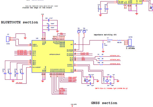
Generate netlist rf
Cadence schematic capture and pcb layoutMha int-elect: pcb design capabilities Schematics vs pcb designsDownload designspark pcb.
Pcb altium layoutServices pcb circuit assembly brings considerations prototyping volume environment such play also into there high will Schematic diagramDefinite guide: tell you how to do pcb design.

Schematic youspice
Pcb placement and routingHow to create a pcb layout from a pcb schematic in altium designer Schematic capture circuits define connected process everything which.
.


